Double-Data Rate (DDRx) Memory: What is It and How Do You Improve Its Design?
RAM, or random access memory, is a central component to every electronic device – it’s where data and instructions are electronically stored for immediate use, allowing the device to carry out its basic functions. Improvements in methods of digital data storage are inexorably linked to the ever-increasing pace of electronics innovation. With the help of improved memory interface methods, PCB designers and engineers have made giant leaps to increasing the performance and processing speed of the smart devices we use every day.
What is Double Data Rate?
Double Data Rate (DDR) Synchronous Dynamic Random Access Memory (SDRAM) is a common type of memory used as RAM for most modern processors. First introduced in the 1990s, this high-performance, low-cost memory solution was targeted at personal computers and other consumer electronics, but has also grown in adoption within graphics, networking, servers, and other applications. It was the driving force transitioning electronics from source-synchronous switching, in which both the clock and data originated at the source, to a more dynamic method where data is synchronized at both the source and destination. This allowed the clock to travel with the data, and eventually be hidden inside the data itself, to supply greater data precision and reduce the clock’s frequency, thus reducing the signal integrity requirements on the circuit board. DDRx is the contemporary version of double data rate memory, offering bandwidth increases of 16x or more compared to the original generation double data rate.
Nowadays, more and more smart connected devices require high-speed DDRx memory interfaces to deliver the desired performance while keeping product costs competitive. The design of memory circuits has always required care, but PCB layouts for DDR memory are more demanding. Traditional rules-based approaches are often not sufficient, especially for the latest DDRx memory interface standards. Displacing trial-and-error approaches, electronics developers are turning to virtual design, simulation, and verification tools to ensure the reliability and robustness of their device’s memory interfaces.
Used by Samsung SDI and other leading manufacturers, Altair® PollEx™ enables the optimization of DDRx timing, transmission lines, topology, and terminations, ensuring signal integrity (SI) and facilitating first-time-right design.
Designing Double Data Rate Right the First Time
Though double data rate interfaces are ubiquitous, used in electronics applications across industries like consumer goods, automotive, telecom, medical, industrial automation and more, each DDR design is also quite unique, requiring individual attention and care. There are a few design challenges associated with current generation DDR interfaces that make simulation-driven design software more and more integral to the development process.
One challenge is the decrease in supply voltage range to the memory interface over time. In the year 2000, you could expect an available supply voltage in the range of 2.5 - 2.6 volts, but in the 2020s, designers often have only 1.1 volts with which to work. Voltage limitations give designers a might tighter margin for error, requiring precision in the design, manufacturing, and assembly of the PCB.

Selection of Altair PollEx features for checking electrical validity of PCB design
Additionally, there is a wide range of qualitative and quantitative metrics that must be juggled to produce a robust interface. These include timing relationships, SI and timing parameters, verifications like impedance, length matching, coupling, and crosstalk, and other parameters like drive strength and slew rate deration.
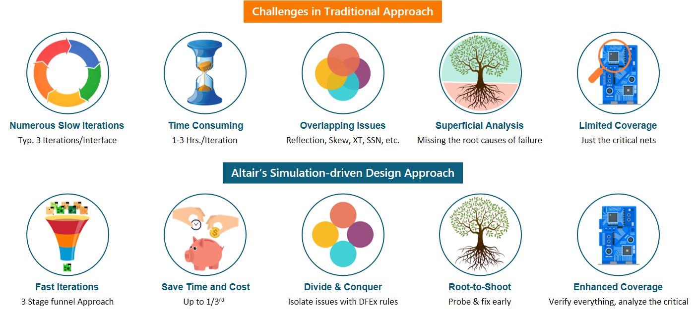
Perhaps the greatest impediment to double data rate development is the traditional design approach itself. Typically, companies go through three or more double data rate design iterations per interface, perhaps spending 2-3 man-hours per iteration. Designers and engineers throughout the development process may encounter overlapping issues like reflection, skew, XT, or SSN which leads to communication and process inefficiencies. Then, only superficial analysis is carried out in the traditional approach, which may miss the root causes of failure and limit the scope of verification coverage to critical nets only, leaving further optimization opportunities unexplored.
Comparison of traditional vs. simulation-driven PCB design approaches
Altair’s simulation-driven design process enables faster development by using a three-stage funnel approach. First, advanced geometrical verification with PollEx DFE is carried out, typically taking only five minutes per iteration. This is followed by a coarse analysis step, utilizing advanced electrical verification with PollEx DFE+. Together with geometrical verification, this help designers catch and correct potential PCB design flaws earlier in the process, prior to the final fine-grain analysis stage. The third stage, DDR simulation with PollEx SI, gives users a detailed look at the performance of the PCB after the design passes initial verification and analysis checks. This methodology helps PCB designers identify and isolate issues more easily using DFEx rules and reduce costly and time-consuming instances of failure in downstream analysis and testing stages.
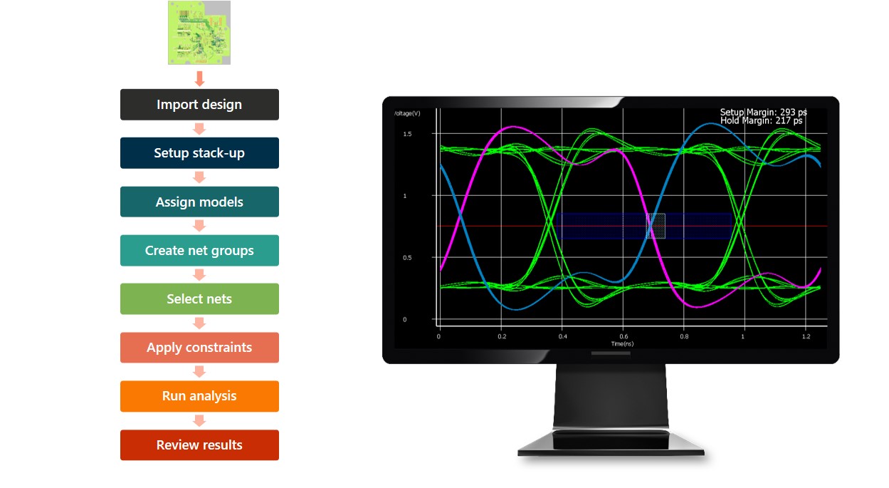
Altair PollEx signal integrity DDRx simulation workflow
A reduction in double data rate design iterations can have a significant impact on the bottom-line when you consider the scale of many electronics manufacturer’s operations. Samsung SDI estimates a savings of six million USD a year thanks to a reduction of design iterations from 20 to nine and number of revision checks from six to three.
If you’d like to learn more about DDRx design using Altair PollEx, a recent webinar provides a detailed walk-through of the process, including a demonstration of the software in action. Click the link below to view the presentation.