
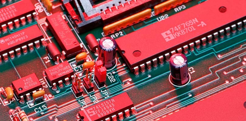
Avoiding the Top 5 Most Common PCB Manufacturing Issues
Process efficiency starts with identifying potential defects and optimizing for manufacturing in the design phase.
 For manufacturers of printed circuit boards (PCBs), one of the most critical questions around a new product introduction (NPI) is, “How do we ensure the quality and consistency of our PCB manufacturing processes?” The discovery of defects can stall development, kick off expensive redesign and testing cycles, and lead to increased warranty claims and damage brand reputation if these issues reach the consumer.
Here are five most common production issues that PCB developers seek to avoid:
Increasingly, electronics developers are turning to simulation-driven design for manufacturing (SDfM) methods to improve their production efficiency and provide solutions to avoid the most common issues plaguing PCB production.
How Does Simulation Improve Production Efficiency?
Injecting simulation into the PCB development process allows design engineers to identify potential PCB manufacturing and assembly issues early in the R&D phase, before they reach downstream validation and physical testing stages. SDfM provides powerful tools to quickly and accurately recognize common PCB defects that would otherwise require extensive manual review or failed lab or field tests to uncover.
Verification checks are a necessary step to reduce PCB manufacturing cost and delivery time. A comprehensive approach involves electrical validity checks (DFE, DFE+, LDFE) and manufacturing validity (DFM, DFA). However, PCB verification tools alone only go so far to improve production efficiency.
Altair PollExTM is a solution that accelerates the development of today’s smart, connected, and tightly packaged electronic products. Used by global industry leaders to improve efficiency, increase performance, enable teamwork, and enhance collaboration, it offers tools for full system analysis that integrate mechanical, thermal, electromagnetic, and embedded code design flow with PCB design.
On top of identifying production issues through verification testing, PollEx offers solutions through DFM/DFA analysis including fabrication, assembly, test, flex/rigid-flex, substrate, and panel features. PollEx also exports PCB manufacturing and validation data to production line machinery for fabrication, assembly, and end-of-line testing. PollEx’s end-to-end electronic systems development tools help reduce PCB manufacturing cost and delivery time by optimizing the PCB design for both function and manufacturability.
Using Validation Checks to Avoid Common PCB Manufacturing Issues
Acid Traps
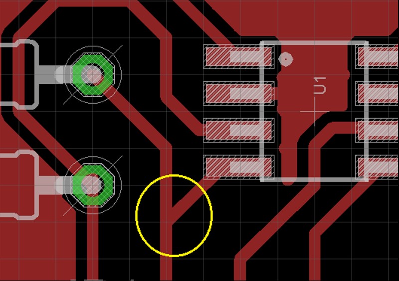 Acid traps are pocket spaces on the PCB, usually sharp corners, in which etching solutions could get trapped. These etching solutions are used to strip excess copper from a board during manufacture. If they are trapped, there is a risk of it tunneling through the board, causing corrosion to the traces and leading to faulty traces.
Acid traps are pocket spaces on the PCB, usually sharp corners, in which etching solutions could get trapped. These etching solutions are used to strip excess copper from a board during manufacture. If they are trapped, there is a risk of it tunneling through the board, causing corrosion to the traces and leading to faulty traces.
Common sources
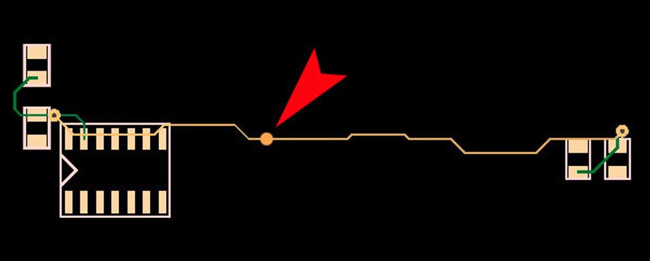
- Trace bending below 90 degrees most likely acts as acid trap during fabrication, specifically before washing when residual acid gets collected in trap area.
- Traces connecting to holes (vias or DIP connections) without teardrops are usually connected at a sharp angle, which could lead to the creation of acid traps.
Verification checks with PollEx
Check for sharp corners for traces: This check looks for patterns that are connected to a pad from a 90-degree angle, helping the user fix routes that will be problematic during etching. This check also helps the user identify if angles are routed in angles other than 45 or 90 degrees by offering a glimpse at all traces flagged as coming into the pad at 90 degrees.
Existence of teardrops: This check helps determine if a component group is lacking a teardrop, especially for DIP type components where the probability of breakout for vias is possible.
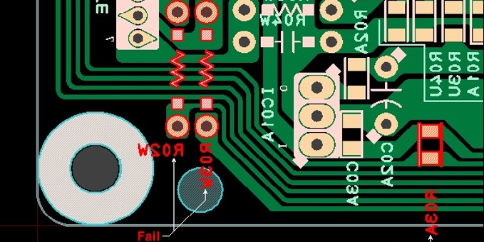
BGA Spacing
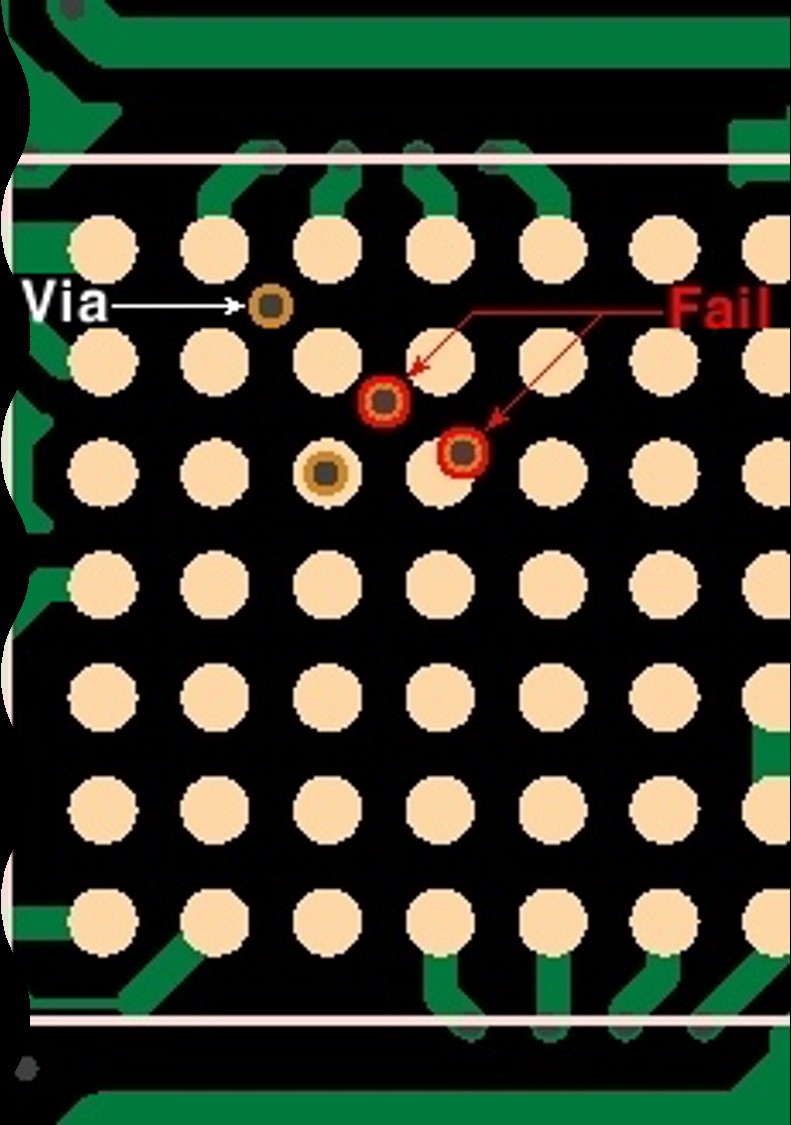 BGA components are a major key to incorporating high-performance ICs into densely populated, complex PCBs. However, there are certain issues that must be considered to ensure proper functionality of the BGA chips. Fixing some of these issues post-manufacturing could prove costly in terms of time and resources.
Common sources
- The majority of the issues with BGAs are associated with pads for the ball grid under the die.
- Proper spacing policy around each BGA pad ensures proper connectivity of the component.
Verification checks with PollEx
Clearance around BGA pads for vias: For the best case BGA routing, the through-hole vias between the BGA pads need to be at the center of four BGA pads. In case this is not achieved, that invites a chance of solder applied to BGA pads to scavenge into the vias, since most BGA pads are non-solder mask defined (i.e., solder mask area is larger than metal pad area).
Tombstone Effect
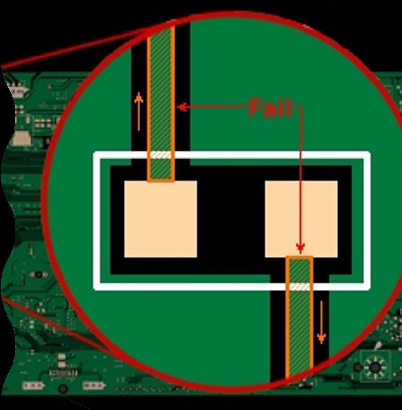 Tombstoning is caused by improper wetting. When the solder paste starts to melt, an imbalanced torque at the ends of the component terminals causes the component to lift from one end.
Common sources
A difference in connected traces of each pad of a two-pin device causes difference in soldering time during the reflowing process, which results in a tombstoned component.
Verification checks with PollEx
Compare the ratio of connected traces: Due to mismatch in heat dissipating traces between two pads, one pad could require more heat to get a proper connection. Therefore, the temperature difference will generate a wetting force imbalance that causes tombstoning. To prevent tombstoning, ensure the ratio between the connected copper at the pads are within the allowable ratio.
Test Point Existence
 A test point is a location within an electronic circuit that is used to either monitor the state of the circuitry or to inject test signals. When designing a PCB, it is important to add fixtures for easy testing of vital nets and components. Such testing setups are essential to test objects with minimum or no modification or rework to the design.
Common sources
- If test points are overlooked in the design stage, equipment errors may be difficult to diagnose during verification in the manufacturing and assembly stage.
Verification checks with PollEx
Check the existence of test points: Typically test points are incorporated in the design for testing critical nets and components which are associated with power delivery or those with difficulty to access, but some areas may be missed. PollEx checks for the existence of test points for specified components and nets.
Visual Features
 When designing a manufacturable PCB, the overlay layers play an important role in the PCB manufacturing process as well as post-manufacturing debug. The overlay layers contain information such as first pin mark, reference names, and component outlines. It is important to make sure information about these overlay layers is accurately represented to avoid any layout discrepancies.
Common sources
- For complicated multi-rowed pin ICs, the first pin indicator helps in case of placement as well debugging.
- For arrays of passive components, the reference names also provide details for cross-probing with the schematic.
- These reference names shouldn’t be placed on top of copper areas such as pads and vias, or underneath a component.
Verification checks with PollEx
Check order of reference names for arrayed passive components: Reference name ordering for arrayed components should be accurate so that they correlate to the correct component to be placed in the array.
Check existence of first pin mark for complex ICs (components with reference name “U#”): Marking the first pin for complex ICs helps to avoid errors during the assembly process which could result in components being placed in an incorrect orientation.
Check for reference names overlapping with other objects (components, pads and holes): Reference name should be avoided placed on certain objects on the board to prevent several issues like ink in holes and ink on traces creating SI and PI issues and ink of solderable surfaces, creating bad solder joints.
Sharing Verification Results
Distributing the results of PCB manufacturing verification tests effectively is equally as important as performing the critical checks themselves. PollEx DFx offers a unique export feature that ensures all information from these checks are distributed seamlessly. With custom Excel formatting, users can export and share detailed information with the peripheral teams.
Altair’s simulation-driven design tools enable teams of specialized engineers to collaborate across all aspects of printed circuit board development from concept to manufacturing. Click here to find out how our products help streamline your process, eliminate design iterations, and reduce time-to-market.