

Accelerate Your PCB Design and Manufacturing Process
The increased digitization and connectivity of society is driving continued growth of the electronic design automation (EDA) tools market, valued at $6.81 billion in 2019 and projected to reach $10.23 billion by 2025, with a compound annual growth rate of 7.8%. EDA is an integral and growing component in the semiconductor and printed circuit board (PCB) design and development process. If we look at the whole PCB market, we can see it is expected to hit $89.7 billion by 2024 due to its role as a key driver for major growth and high demand from major industries such as consumer electronics, Internet of Things (IoT), and automotive.
PCB trends and challenges today
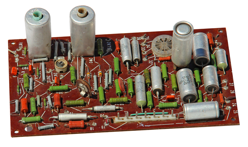
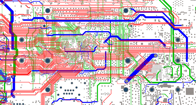
The density in PCBs during the last 15 to 20 years has dramatically increased. But it is not only the density that is changing - PCB systems are getting smaller and smaller, and with increased speeds and frequencies like with 5G (which translate not just into more data, but more interferences and losses as well). Voltages are increasing to 48 volts and to hundreds of volts due to requirements for electric vehicles. Standardization, RoHS “green” PCBs, globalization, and supply chain control are also growing aspects in this industry.
This increasing complexity requires highly specialized engineer profiles spanning across various areas of expertise, involved in the design and manufacturing of PCBs. Whereas in the 80’s, we could talk about three different types of profiles, today there are teams with over 10 different profiles. How can these teams of engineers best communicate and work effectively during the development of a PCB? Also take into consideration the many sequential design flows - each of which involve multiple processes, and use a different software tool and library per process! As you can imagine, the scalability and efficiency of these processes are major challenges for those companies who are competing to get their products to market faster while staying cost-efficient.
Evolution of PCB design complexity over time until today (left to right)
How can innovative organizations go to market faster while reducing development and manufacturing costs?
Having a solution to reduce the number of iterations from PCB to manufacturing that also considers the design and manufacturing supply chains, is key. And luckily, this is where our comprehensive EDA software solution, Altair PollEx™, comes into play.
Altair PollEx is already the trusted go-to solution for many key global industry leaders such as Samsung and LG, as it enables them to:
Do you want to learn how you can leverage the benefits of Altair PollEx in your design and manufacturing process? We invite you to join other industry leading electronic organizations on the path forward towards strategic scalability and efficiency.
Join our free live webinar on March 25 to learn more.
PCB trends and challenges today
The density in PCBs during the last 15 to 20 years has dramatically increased. But it is not only the density that is changing - PCB systems are getting smaller and smaller, and with increased speeds and frequencies like with 5G (which translate not just into more data, but more interferences and losses as well). Voltages are increasing to 48 volts and to hundreds of volts due to requirements for electric vehicles. Standardization, RoHS “green” PCBs, globalization, and supply chain control are also growing aspects in this industry.
This increasing complexity requires highly specialized engineer profiles spanning across various areas of expertise, involved in the design and manufacturing of PCBs. Whereas in the 80’s, we could talk about three different types of profiles, today there are teams with over 10 different profiles. How can these teams of engineers best communicate and work effectively during the development of a PCB? Also take into consideration the many sequential design flows - each of which involve multiple processes, and use a different software tool and library per process! As you can imagine, the scalability and efficiency of these processes are major challenges for those companies who are competing to get their products to market faster while staying cost-efficient.
 |
 |
How can innovative organizations go to market faster while reducing development and manufacturing costs?
Having a solution to reduce the number of iterations from PCB to manufacturing that also considers the design and manufacturing supply chains, is key. And luckily, this is where our comprehensive EDA software solution, Altair PollEx™, comes into play.
Altair PollEx is already the trusted go-to solution for many key global industry leaders such as Samsung and LG, as it enables them to:
- easily and quickly visualize, review and compare PCB designs coming from major ECAD systems, while securely sharing such designs
- significantly save costs by detecting manufacturability, assembly and electrical defects and faults early in the design process
Do you want to learn how you can leverage the benefits of Altair PollEx in your design and manufacturing process? We invite you to join other industry leading electronic organizations on the path forward towards strategic scalability and efficiency.
Join our free live webinar on March 25 to learn more.


